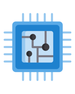
Silicon Wafers

Silicon wafers

Sikata is a leading sourcing and trading company specializing in high-purity silicon wafers. We bridge the gap between top-tier manufacturers and businesses seeking reliable and cost-effective silicon materials. Our commitment to quality, innovation, and sustainability sets us apart in the industry.

Sikata is a trusted global supplier of high-quality silicon wafers, catering to the semiconductor, photovoltaic, and microelectronics industries. With a strong network of manufacturing partners and an unwavering commitment to excellence, we provide a comprehensive range of prime, test, and reclaimed wafers tailored to meet the exacting standards of our clients.

Backed by industry expertise and a deep understanding of market dynamics, we ensure a seamless supply chain, competitive pricing, and stringent quality control. Our solutions support cutting-edge research, advanced manufacturing, and technological innovation across diverse applications.

At Sikata, we prioritize reliability, precision, and customer-centric service. Whether you require wafers for semiconductor fabrication, MEMS production, or R&D initiatives, we are dedicated to delivering superior products and tailored solutions that drive progress.

Partner with us to power the future of technology.

Sustainability Commitment

Eco-Friendly Sourcing:

Partnering with manufacturers who prioritize sustainable production.

Wafer Recycling Services:

Reducing semiconductor waste through reclaiming initiatives.

Energy Efficiency:

Promoting solar-grade silicon to support renewable energy solutions.

Introduction

A silicon wafers are thin, circular slice of silicon crystal used as a substrate in the fabrication of semiconductor devices like integrated circuits (ICs), solar cells, and microelectromechanical systems (MEMS). Silicon wafers are a critical component in the electronics and renewable energy industries due to silicon’s unique properties, such as its semiconducting nature and abundance in the Earth’s crust. Below is a comprehensive overview:

1. Composition and Properties

Material:

Pure silicon, often doped with impurities like phosphorus, boron, or arsenic to alter its electrical properties.

Crystal Structure:

Single-crystal silicon with a diamond cubic lattice structure.

Thermal Properties:

High thermal conductivity and stability.

Electrical Properties:

Intrinsic silicon has low conductivity, but doping makes it a good semiconductor.

The production of silicon wafers involves several steps:

A. Silicon Extraction

Silicon is derived from silica (SiO₂), commonly found in sand or quartz.

The silica is refined into metallurgical-grade silicon, which is then purified further into electronic-grade silicon.

B. Crystal Growth

Czochralski (CZ) Process: A seed crystal is dipped into molten silicon, and the silicon crystallizes around the seed as it is slowly pulled and rotated.

Float Zone (FZ) Process: A zone-melting technique used to produce high-purity wafers with fewer defects.

C. Wafer Slicing

The silicon ingot is sliced into thin wafers using a wire saw.

The thickness depends on the application (e.g., solar panels use thinner wafers than ICs).

D. Wafer Polishing

Wafers are polished to achieve a smooth, defect-free surface suitable for photolithography.

E. Doping

Dopants are introduced to modify the wafer’s electrical properties, creating either n-type (negative charge carriers) or p-type (positive charge carriers) silicon.

F. Etching and Cleaning

Chemical etching removes surface damage from slicing, and cleaning eliminates contaminants.

Types Of Silicon Wafers

  • Monocrystalline Wafers:

    Single crystal, high purity, used for ICs and high-efficiency solar cells.

  • Polycrystalline Wafers:

    Multiple small silicon crystals, used in cost-effective solar cells.

  • Epitaxial Wafers:

    Thin layers of silicon grown on a substrate for advanced semiconductor devices.

  • SOI (Silicon-on-Insulator) Wafers:

    A layer of silicon dioxide insulates the active silicon layer, used for low-power electronics.

Size's

WordPress Table Plugin

Applications

  • Semiconductors:

    Semiconductors:

    Used as substrates for manufacturing ICs, microprocessors, and memory chips.
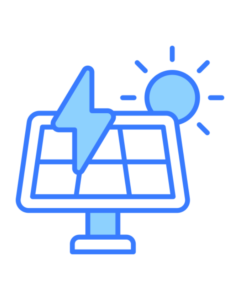
  • Solar Cells:

    Solar Cells:

    Silicon wafers form the basis of photovoltaic cells in solar panels.

  • MEMS Devices:

    MEMS Devices:

    Used in sensors
    (e.g., accelerometers, gyroscopes).
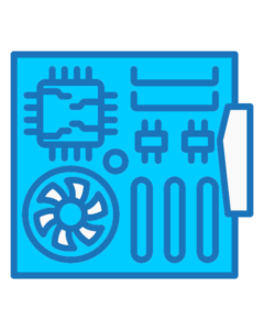
  • Power Electronics:

    Power Electronics:

    High-purity wafers are essential for devices like diodes and transistors.
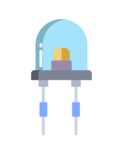
  • LEDs:

    LEDs:

    Substrate for LED fabrication.

© 2025 Powered by ARDT